This project is part of the autonomous underwater vehicle I’m building in Paris. An AUV, or autonomous underwater vehicle, is basically a robot submarine: a compact system that has to balance power delivery, data integrity, sealing, vibration, and electromagnetic noise in a very small space.
For this payload interface board, I designed a custom PCB that connects the external tether to the Jetson compute unit inside the vehicle. The goal was to move power and high-speed USB data reliably through a harsh underwater environment while protecting the electronics from thruster noise, ESD, and voltage spikes.
Objective: Design a custom, impedance-controlled interface to reliably deliver power and high-speed data between an external tether and the internal NVIDIA Jetson compute unit.
Operating Environment: Custom RC Autonomous Underwater Vehicle (AUV) rated for 15-meter depths, utilizing 3D-printed end caps. The board is designed to reject heavy EMI from the thruster motors and protect sensitive silicon from voltage spikes.
Schematic
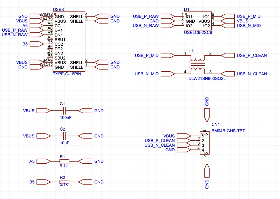
Signal Protection (USBLC6-2SC6): Implemented a flow-through TVS diode array on the raw USB inputs to clamp high-voltage transients and ESD events before they reach the Jetson.
EMI Rejection (Common-Mode Choke): Placed a 90Ω common-mode choke in series with the data lines to filter out high-frequency noise generated by the AUV’s thruster ESCs.
Power Filtering: Wired 100nF and 10uF bulk decoupling capacitors in parallel along the VBUS line to smooth out power delivery and prevent brownouts during high-current payload draw.
PCB
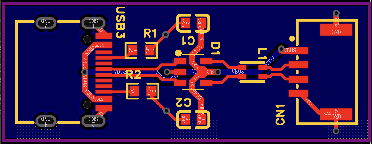
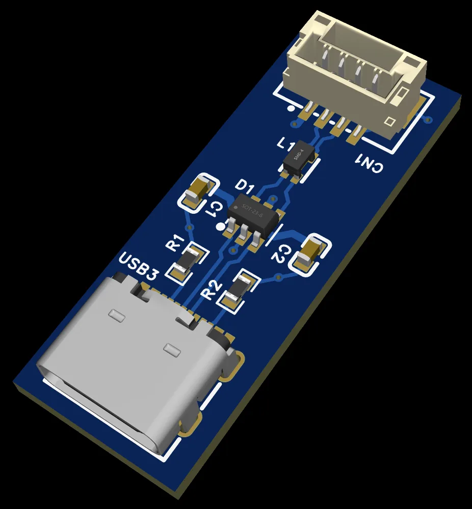
USB-C Connector ➔ ESD Diode ➔ Common Mode Choke ➔ JST-GH Connector
Strict 90Ω Differential Routing: USB_P and USB_N were routed as a tightly coupled differential pair to maintain a 90Ω impedance.
Zero-Via Data Path: To preserve signal integrity and avoid impedance bumps, the data traces run exclusively on the top layer from the Type-C receptacle directly into the JST connector.
Strategic Power Routing: To allow the data lines a perfectly straight path, the VBUS line drops to the bottom layer via and travels cleanly underneath the flow-through diode package, completely eliminating trace crossovers.
Grounding: Implemented a continuous solid copper ground pour with proper edge pullback to prevent manufacturing delamination.
Conclusion
This interface board is a small example of the kind of engineering I enjoy most: compact, practical hardware that has to perform in a hostile real-world environment. The final result is simple, robust, and ready to sit inside the AUV without wasting space or compromising signal integrity.